Research
Interfaces and boundaries between materials, phases, and structural motifs are ubiquitous in our natural and manufactured world. Changes in the atomic and electronic structure at interfaces lead to unique properties such as modified excited state lifetimes, charge transport mechanisms, and interfacial electronic states. In materials, boundaries and interfaces can create unique electronic states that modify charge transfer or facilitate charge recombination. This influences material functionality, particularly in non-equilibrium systems such as photovoltaics, electrochemical cells, and heterogeneous catalysis. In my research group, we aim to investigate how the nanoscale and mesoscale structure of materials, including the presence of grain boundaries and interfaces, influences electronic structure, excited state dynamics, chemical reactivity, and their ultimate functionality.
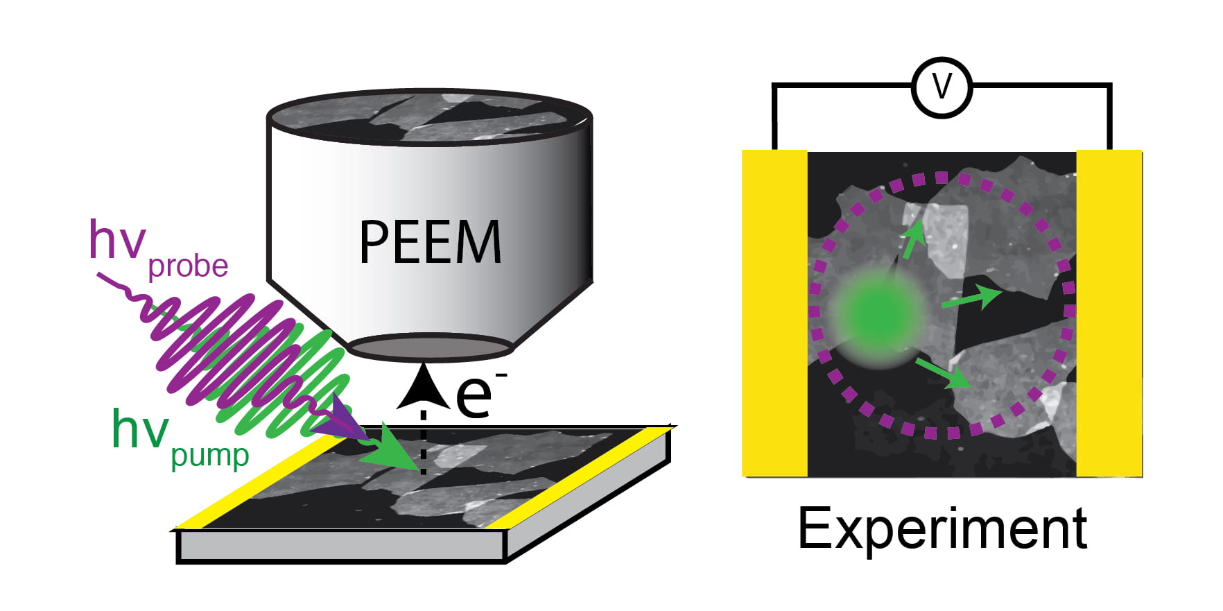
Time-resolved PEEM will be used to image the ultrafast dynamics of charge transport on the nanoscale. The transport of carriers excited by a pump pulse (green) will be probed as a function of time with a probe pulse (purple). Image adapted from Nat. Rev. Mater 2, 16098 (2017).
In polycrystalline and heterogeneous materials, electronic states and excited state dynamics can be strongly dependent upon the nanoscale and mesoscale structure due to variations in molecular packing, alignment, material thickness, and grain boundaries. Grain-boundaries can, for example, inhibit exciton formation, modify photoluminescence, or disrupt phonon and polaron transport, thereby fundamentally changing a material’s functionality. A detailed understanding of the energetics and dynamics of materials on the nanoscale is therefore critical to understand the photophysics and functionality of a bulk polycrystalline material. However, resolving the nano and mesoscale electronic structure and dynamics of heterogenous materials requires spatial resolution on the order of 10s of nanometers and crystalline grain sizes can range from nanometers to 10s of microns, smaller than the diffraction limit of conventional optical spectroscopies. Electron microscopy has a much higher spatial resolution than optical microscopy because the diffraction limit of an electron is smaller than that of a photon. The group will combine time-resolved spectroscopy with a photoemission electron microscope in order to directly image the ultrafast dynamics of materials with a spatial resolution of 10s of nm, determining the interplay between structure, dynamics, and function in polycrystalline and heterogeneous materials.
Using our novel time-resolved photoemission electron microscope with near-normal incidence laser excitation and sample cooling from 30 K to room temperature we are investigating a wide range of heterogenous materials from 2D black phosphorous, covalent organic frameworks, and molecular electronics to hybrid light-matter materials.
The properties and dynamics of buried interfaces are at the heart of material and energy transformation, ranging from energy transfer between a battery electrode and a solid or liquid electrolyte to the surface chemistry that can occur at a solid-liquid interface. It is well known that the surface properties of materials can be distinct from those of a bulk material. At material interfaces unique surface electronic states can exist, band-bending can alter the energy of conduction and valence bands relative to the Fermi level, and even a material’s crystal structure can be significantly modified.
These interfacial electronic states are often the “gatekeepers” for charge transfer and reactivity at buried interfaces but selectively investigating their electronic structure and ultrafast dynamics has proved difficult due to a dearth of experimental methods to probe them selectively. The group is developing a time-resolved phase-stabilized electronic sum-frequency generation spectrometer to probe the electronic structure and ultrafast dynamics of buried interfaces in situ.
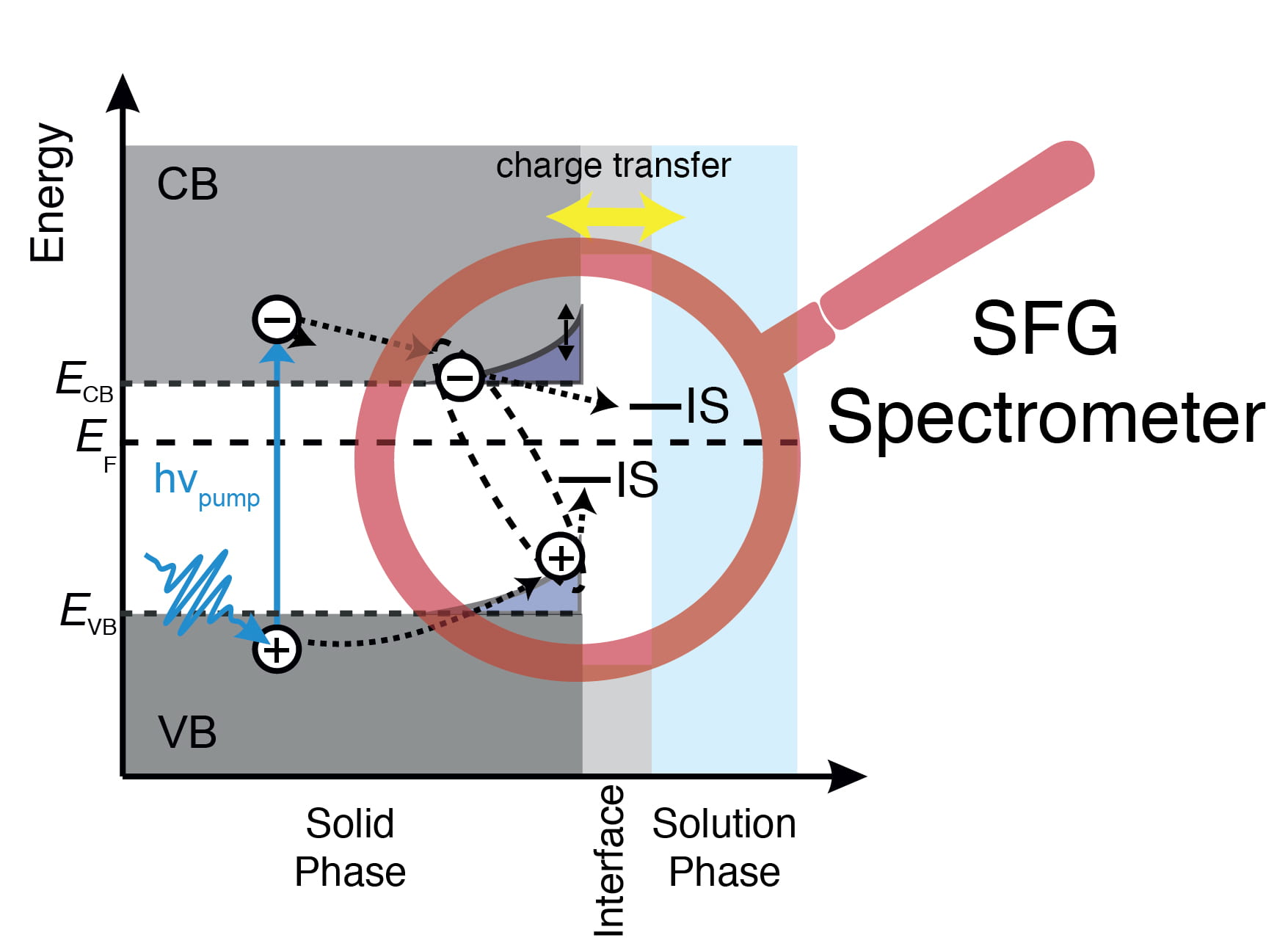
Time-resolved SFG spectroscopy will be used to selectively probe, for example, the electronic structure and dynamics of a solid liquid interface and the role of interface states (IS) the reactivity of the interface.
Funding
We are grateful for funding from the following sources: